Electrically isolated (GI) gate drivers play a crucial role in optimizing the performance of silicon carbide (SiC) MOSFETs, especially in addressing the growing demands of electrification systems. As the global reliance on electricity deepens across industrial, transportation, and consumer products, SiC technology stands out for its ability to enhance efficiency and reduce system size. This article is the first in a series, introducing the basics of MOSFETs, gate drivers, and electrically isolated gate drivers, along with a guide for selecting electrically isolated gate drivers.
As our world becomes increasingly electrified, the demand for electricity to power various devices and systems continues to grow. For instance, in the automotive industry, we see more and more electrical systems being integrated into vehicles to ensure safety and provide convenience for users. The widespread transition from vehicles relying entirely or partially (hybrid) on internal combustion engines to fully electric vehicles and even fuel cell vehicles further amplifies this trend.
To meet the growing power demands of devices and provide greater overall power, electrical systems are evolving toward higher operating voltages and frequencies. This shift aims to improve efficiency, accelerate charging speeds, and minimize the size and weight of conductors and other system components.
Many aspects of this transition can be better achieved through the adoption of SiC devices, which can handle higher power and temperatures compared to traditional silicon (Si) devices.
However, SiC MOSFETs cannot function properly without gate drivers. Therefore, pairing each power switch (GaN, MOSFET, and IGBT) with an electrically isolated gate driver is more effective. Electrically isolated gate drivers possess characteristics that are critical for optimizing the performance of SiC MOSFET devices. In terms of performance optimization, electrically isolated gate drivers help reduce energy losses through efficient switching. onsemi's latest devices reduce external components through built-in negative bias, thereby saving costs.
Understanding Gate Drivers
A gate driver is a power amplifier that receives low-power input signals from a controller IC and generates appropriate high-current gate drive signals suitable for power switching devices such as MOSFETs or IGBTs.
SiC and Si power MOSFETs are voltage-controlled devices used as switching elements in power circuits, motor drives, and other systems. The gate is an electrically isolated control terminal formed by a gate capacitance, which must charge and discharge each time the MOSFET turns on or off. Moreover, this gate capacitance cannot instantaneously change its voltage, leading to switching losses. The other two terminals of the MOSFET are the source and the drain.
Gate Driving: SiC Turn-On
Generally, the turn-on process of SiC devices can be broken down into the following four distinct time intervals, as shown in Figure 1 below:
-
Time Interval 1: The gate driver increases the gate-to-source voltage (VGS) from 0 V to the gate-to-source threshold voltage (VGS(TH)). During this period, the gate drive current (IG) momentarily reaches its peak. The drain-to-source voltage (VDS) remains unchanged. At this point, no drain current (ID) flows.
-
Time Interval 2: The gate driver continues to increase the gate-to-source voltage (VGS) to the Miller plateau region. The gate drive current (IG) decreases. The drain-to-source voltage (VDS) remains unchanged. At this point, the drain current (ID) begins to increase.
-
Time Interval 3: The gate driver maintains the gate-to-source voltage (VGS) within the Miller plateau region. The gate drive current (IG) stabilizes. The drain-to-source voltage (VDS) begins to decrease. At this point, the drain current (ID) reaches its maximum value.
-
Time Interval 4: The gate driver increases the gate-to-source voltage (VGS) to its maximum value, typically 18 V. At this point, the gate drive current (IG) drops to 0 A. The drain-to-source voltage (VDS) remains at a low level. At this point, the drain current (ID) reaches its maximum value, while the on-resistance (RDSON) is at its minimum level.
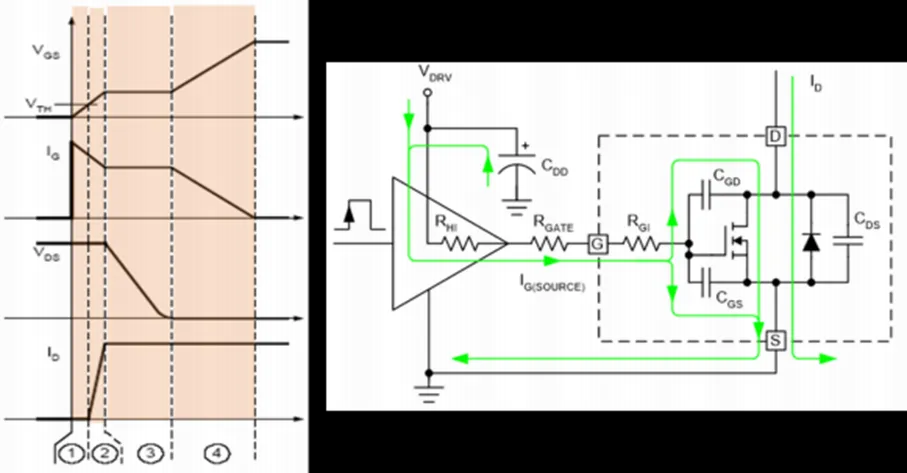
Figure 1. SiC Turn-On
Gate Driving: SiC Turn-Off
Similarly, the turn-off process of SiC devices can also be broken down into the following four distinct time intervals, as shown in Figure 2 below:
-
Time Interval 1: The gate driver decreases the gate-to-source voltage (VGS) from 18 V to the Miller plateau region. The gate drive current (IG) momentarily reaches its peak. The drain-to-source voltage (VDS) remains at a low level. At this point, the drain current (ID) continues to flow.
-
Time Interval 2: The gate driver maintains the gate-to-source voltage (VGS) within the Miller plateau region. The gate drive current (IG) stabilizes. The drain-to-source voltage (VDS) begins to rise. At this point, the drain current (ID) continues to flow.
-
Time Interval 3: The gate driver decreases the gate-to-source voltage (VGS) to the gate-to-source threshold voltage (VGS(TH)). The gate drive current (IG) decreases. The drain-to-source voltage (VDS) is now high. At this point, the drain current (ID) decreases.
-
Time Interval 4: The gate driver decreases the gate-to-source voltage (VGS) to its minimum value, typically 0 V or even lower to -5 V. At this point, the gate drive current (IG) drops to 0 A. The drain-to-source voltage (VDS) remains high. At this point, the drain current (ID) is 0 A, while the on-resistance (RDSON) reaches its maximum level.

Figure 2. SiC Turn-Off
The Importance of Isolation
As the battery voltage of electric vehicles has risen to 800 V or higher, the importance of electrically isolated gate drivers has become increasingly evident. Electrically isolated gate drivers feature an isolation structure between the primary side (connected to the low-voltage system) and the secondary side (connected to the power stage). This allows the low-voltage system to safely withstand high-voltage surges, preventing damage to equipment or harm to humans. Additionally, electrical isolation provides protection against significant potential differences. Therefore, electrically isolated gate drivers are better suited for driving SiC MOSFETs compared to non-isolated gate drivers.
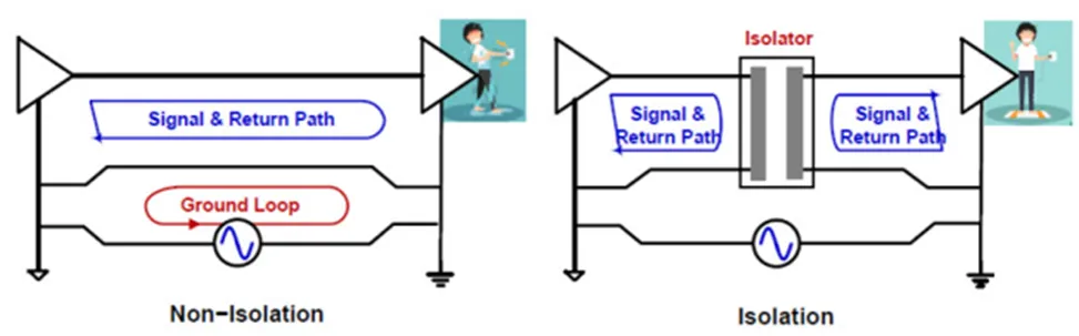
Figure 3. Non-Isolated vs. Isolated Comparison
Electrically Isolated Drivers in High-Frequency SiC Systems
When deploying high-frequency SiC systems, electrical isolation (GI) is particularly important. In addition to providing voltage surge protection during high-frequency operation, electrically isolated gate drivers protect intelligent and expensive low-voltage systems, such as controller ICs, within the physical isolation structure between low-voltage and high-voltage system areas.
Electrical isolation also ensures that devices can withstand significant ground potential differences and reduces the risk of destructive ground loops in high-energy or physically distant circuits.
Parasitic Turn-On
Due to very high di/dt, excessive ringing may occur when the gate driver reaches the minimum gate-source voltage. Additionally, PCB layout and component packaging can increase parasitic capacitance and inductance, leading to inductive kickback during the turn-off process. These inductive kickbacks may inadvertently trigger the threshold voltage (Vgs(Th)), causing unintended turn-on during what should be the off-state, potentially leading to catastrophic consequences.
For example, consider the following scenario in a half-bridge application: when the low-side switch is turning off and the high-side switch is preparing to turn on, the low-side switch may inadvertently turn on due to inductive kickback (triggering VGS(TH)). This can result in both the high-side and low-side switches conducting simultaneously (shoot-through current), potentially causing a direct short circuit between the high-voltage rail and ground, damaging the MOSFET. A highly effective solution to this issue is to swing the voltage below 0 V during turn-off, reducing it to -3 V or even -5 V, thereby providing sufficient margin to prevent unintended triggering of VGS(TH) due to inductive kickback.
EOFF Loss Reduction by 25%
In Figure 4 below, the x-axis represents the negative bias turn-off voltage ranging from 0 V to -5 V, while the y-axis represents switching losses (microjoules, μJ). This demonstrates the second advantage of negative bias turn-off, which is the significant reduction in EOFF switching losses. In fact, when driving onsemi's second-generation "M3S" series SiC MOSFETs (designed for high-frequency switching applications), reducing the turn-off voltage from 0 V to -3 V can lower switching losses by up to 100 μJ. Specifically, turn-off losses decrease from 350 μJ at 0 V to 250 μJ at -3 V negative bias turn-off, representing a 25% reduction in turn-off losses.
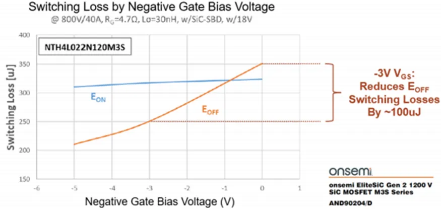
Figure 4. Negative Gate Bias
Electrically Isolated Gate Driver Selection Guide
When evaluating electrically isolated gate drivers for your application, consider the following factors:
General Selection Guide for Low-Voltage and High-Voltage Systems
In systems with lower operating voltages, switching elements can be directly connected to the controller as long as the controller's voltage tolerance is within the permissible range. However, many systems include both high-voltage and low-voltage regions. These systems require converting high-voltage DC to low-voltage DC, AC to DC, and so on. Various topologies, such as half-bridge, full-bridge, boost, and buck, are used in power conversion. The functional modules used for power conversion are referred to as "converters," and gate drivers are common components in most power converters. Since control circuits operate at low voltages, the controller cannot provide sufficient power to quickly and safely turn power switches on or off. Therefore, the signals from the controller are sent to the gate driver, which can handle higher power and drive the MOSFET gate as needed.
When operating in high-power or high-voltage applications, components in the circuit are subjected to large voltage offsets and high currents. If the power MOSFET leaks current to the control circuit, the high voltage and current involved in the power conversion circuit can easily damage the transistors, causing severe breakdown of the control circuit. Therefore, in high-power applications, electrical isolation must be implemented between the input and output of the gate driver to protect users and any connected devices.
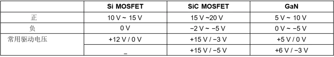
Gate Drive Voltage Ranges for SiC, Si, and GaN MOSFETs
Within the gate drive voltage ranges for SiC, Si, and GaN MOSFETs, the operating voltage of the converter is determined by the specifications of the switching elements, so it is essential to ensure that the converter's output voltage does not exceed the maximum gate voltage of the switching elements.
The positive gate drive voltage should be high enough to ensure the gate is fully turned on. At the same time, the drive voltage should not exceed the absolute maximum gate voltage. Driving Si MOSFETs typically requires 12 V or higher, while driving SiC MOSFETs requires 15 V or higher, and driving GaN FETs requires at least 5 V.
When the gate voltage is 0 V, it satisfies the turn-off conditions for all devices. Typically, silicon MOSFETs do not require negative bias gate drive, but SiC and GaN MOSFET devices sometimes use negative bias gate drive. It is strongly recommended to use negative bias gate drive for SiC and GaN MOSFETs in switching applications because, during high di/dt (rate of current change) and dv/dt (rate of voltage change) switching processes, parasitic inductance and capacitance introduced by PCB layout and component packaging can cause ringing in the gate-source drive voltage of the power transistor.
The table below lists the gate drive voltage ranges suitable for each type of switching device.
Gate Drive Voltage Ranges