
1. Introduction
When debugging the E3 chip, using the IAR integrated development environment is an efficient and convenient method. This article will explain how to debug the E3 chip using IAR, including how to view the values of E3 registers, set data breakpoints, and dynamically observe variable values.
2. Viewing E3 Register Values Using IAR
Method 1:
View the corresponding register values through the Memory Window:
- First, obtain the register address:
Retrieve the register value from the RM, obtain the peripheral base address through the Memory Map, and then locate the specific description of the peripheral register in the corresponding section to find the offset address of the desired register. Alternatively, you can find the base address and offset in the program, such as in xxxx_reg.h.
Example: How to obtain the address of the GPIO_L2 multiplexing register?
① Find the base address: The peripheral module controlled by GPIO_L2 is PINCTRL_AP, and its base address is 0xF30E0000.
② Find the offset address of the corresponding register: The offset address of PIN_MUX_GPIO_L2 is 0x2008.
Thus, the address of the GPIO_L2 multiplexing register can be calculated as 0xF30E0000 + 0x2008 = 0xF30E2008
-
Open the IAR menu bar and navigate to View->Memory->Memory1. A Memory1 window will appear. Enter the address found in step 1 into the Go to field and press Enter to jump to the corresponding register, where the cursor will appear.
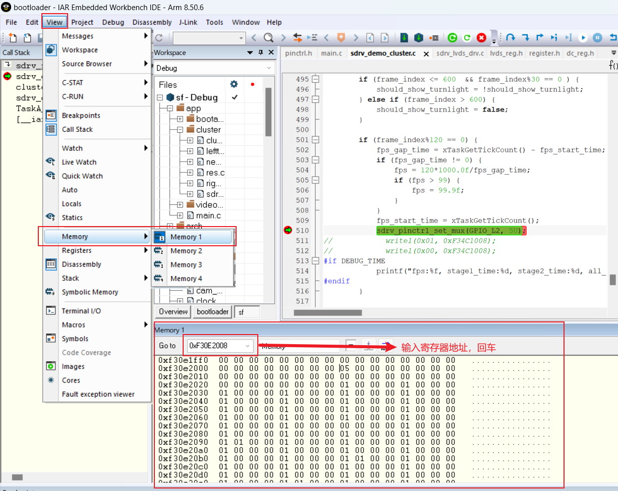
Note that the E3 register storage uses little-endian format. For a 32-bit register containing byte4, byte3, byte2, and byte1, the data observed in memory is byte1, byte2, byte3, byte4. For 0xF30E2008, the actual value is 0x00000005, meaning the GPIO_L2 multiplexing value is 5.
Method 2:
The previous method requires manual lookup and calculation to read register values. By configuring the .ddf file in the IAR Debugger settings, you can achieve graphical display of the corresponding register data:
Taking E3340 as an example:
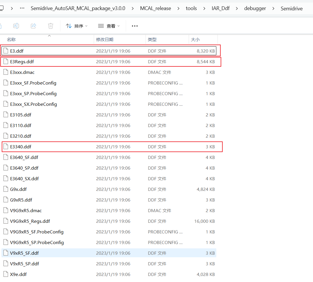
① Locate the files E3.ddf, E3Regs.ddf, and E3340.ddf in MCAL _release\tools\IAR_Ddf\debugger\Semidrive. If using the SSDK project, place these three files in a fixed path within the SSDK project.
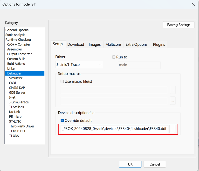
② In Options-->Debugger--Device description file, add the E3340.ddf register file:
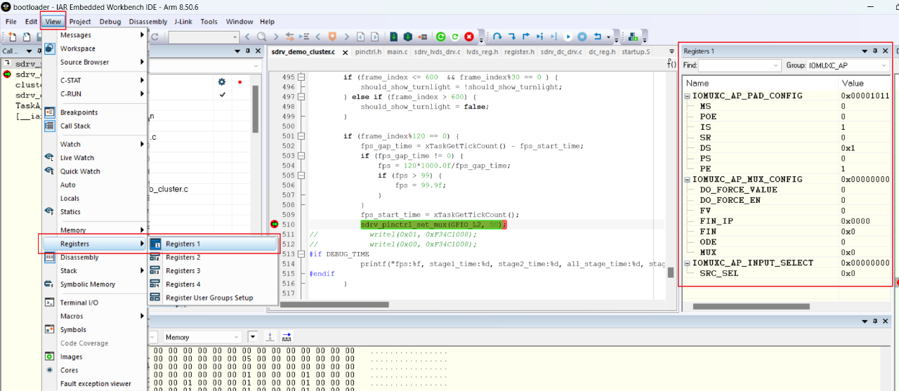
You can then view the defined register values in the IAR menu bar under View->Registers->Registers 1. Note: Registers not defined in the register description file cannot be viewed.
3. Setting Data Breakpoints
In program pause mode, right-click on the byte position of the corresponding register and select Set Data Breakpoint to set a breakpoint that triggers when data is read or written. This allows you to observe the code location where the breakpoint is triggered.
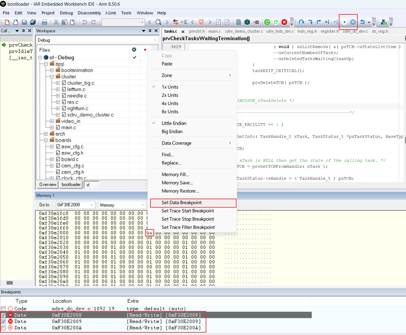
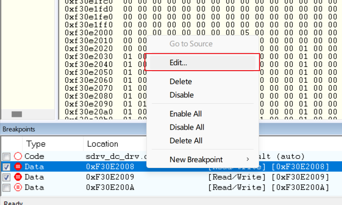
By right-clicking on the breakpoint under Breakpoints and selecting Edit..., you can configure the breakpoint's properties.
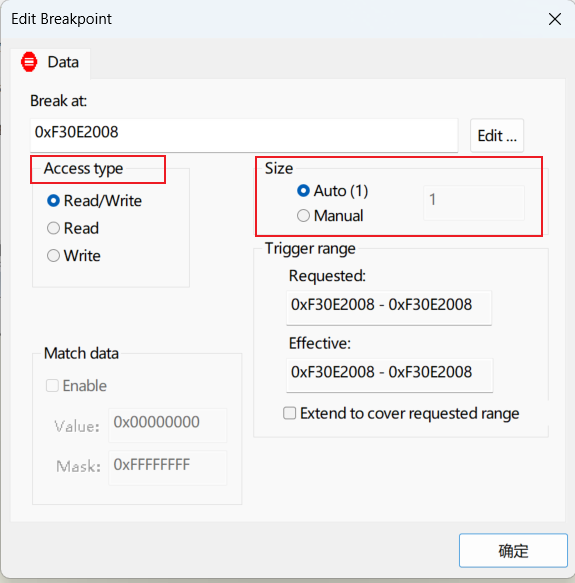
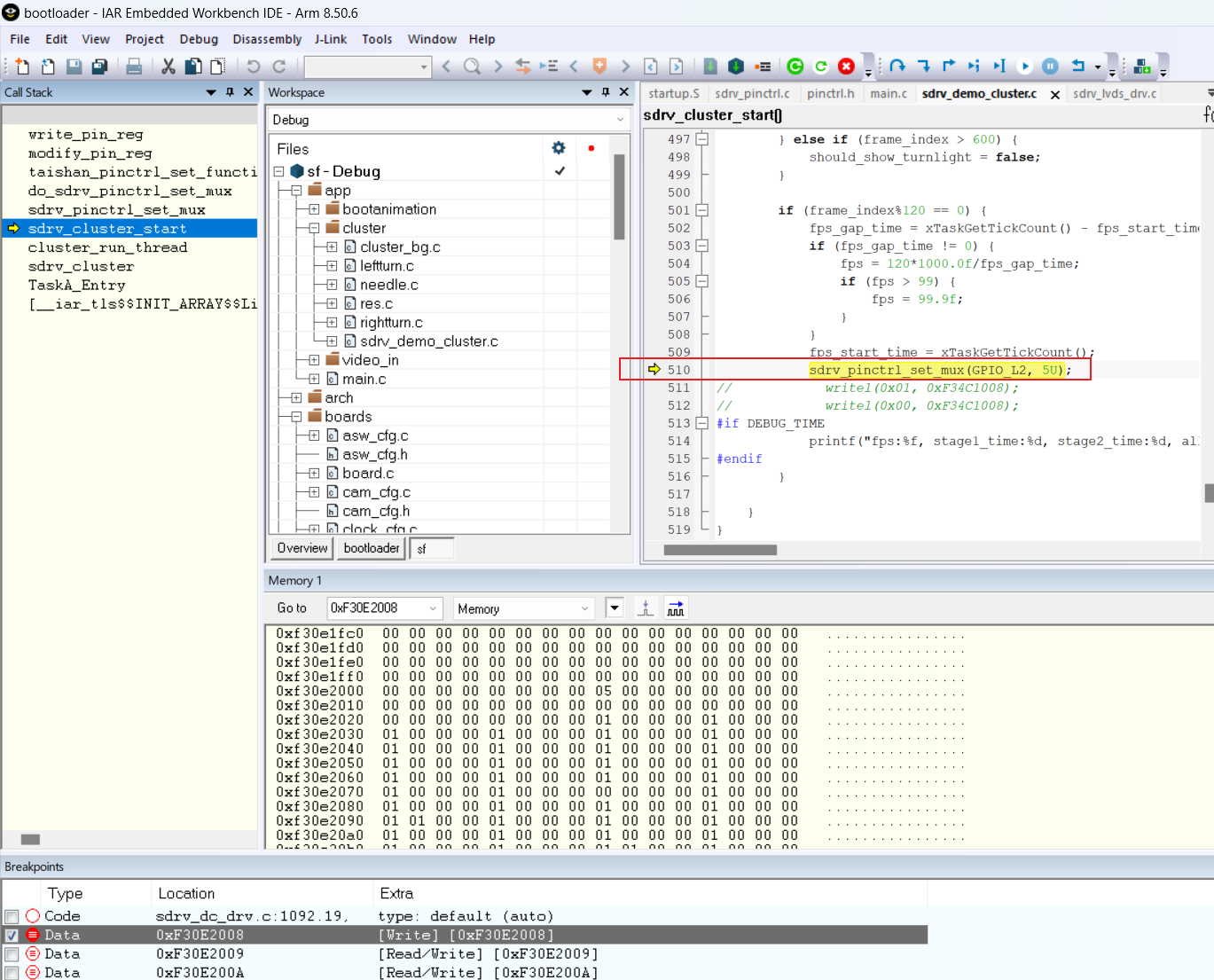
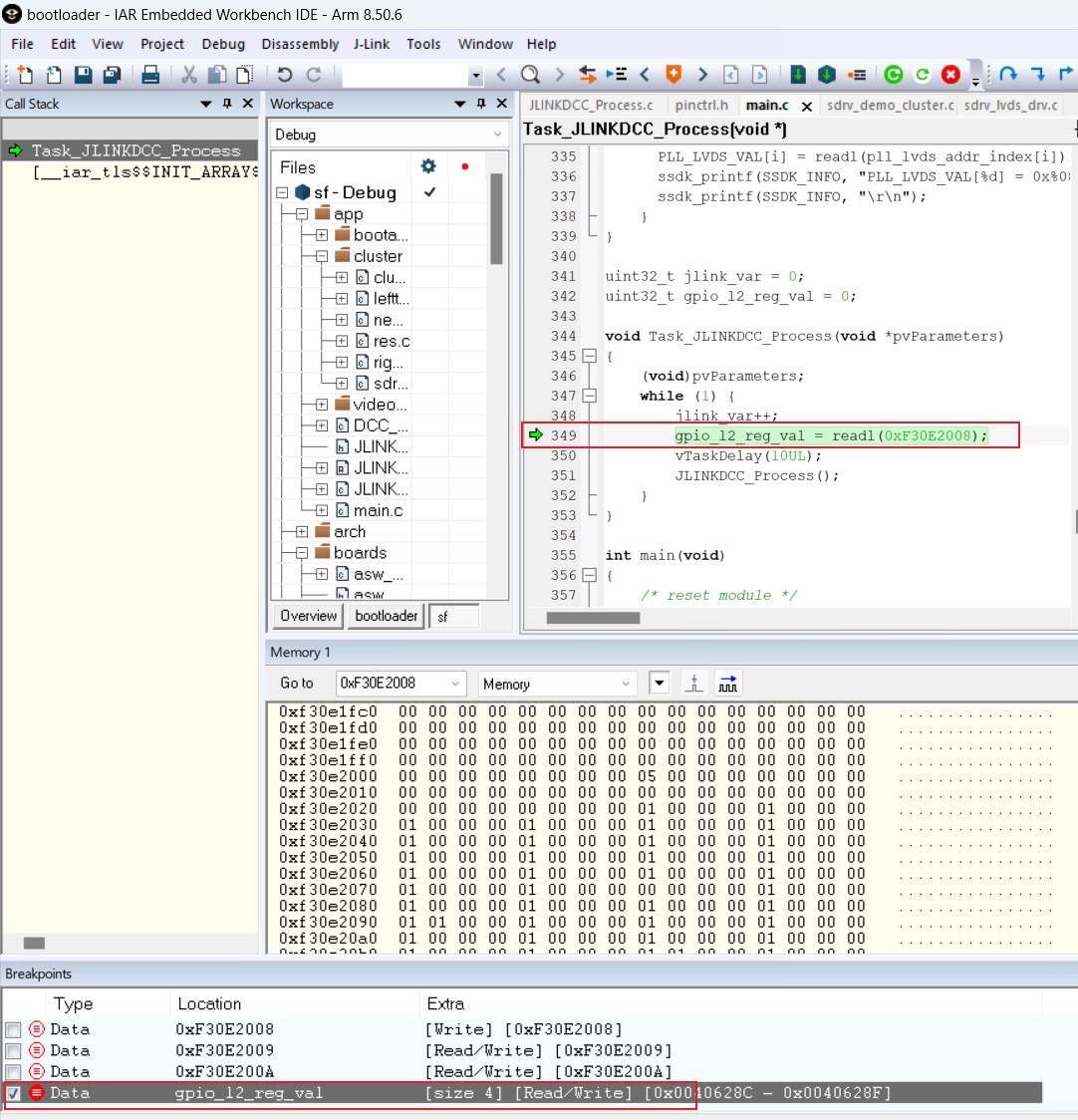
For example, when setting a write breakpoint for 0xF30E2008, a data interrupt is triggered. You can use the Call Stack to identify which operation caused the write to this register.
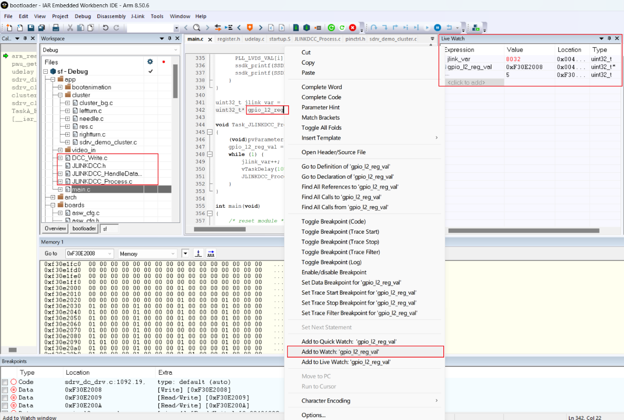
Similarly, for global variables like gpio_12_reg_val, you can set data breakpoints to observe when the data is read or written.
4. How to Dynamically View Variable Values
The methods mentioned in Section 2 are for statically viewing register values. If you want to dynamically view register values or other global and static variables during program execution, you can use JLink's DDC to communicate bidirectionally with the CPU. Through the JTAG/SWD interface, you can communicate with the CPU without stopping the program.
-
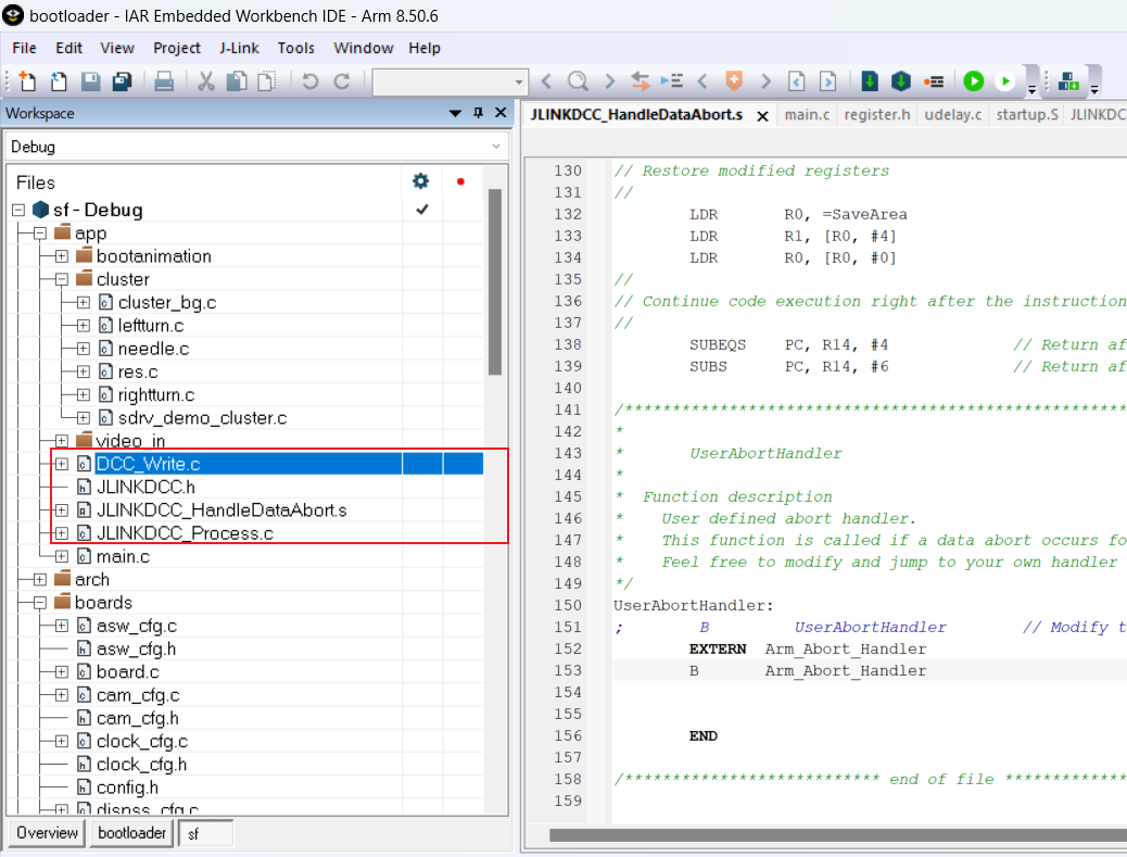
In the IAR installation directory: C:\Program Files (x86)\IAR Systems\Embedded Workbench 8.4\arm\src\debugger\DCC, copy the following files to the project directory to be debugged and add these files to the project compilation.DCC_Write.c (optional)JLINKDCC.h (mandatory)JLINKDCC_HandleDataAbort.s (optional)JLINKDCC_Process.c (mandatory)
-
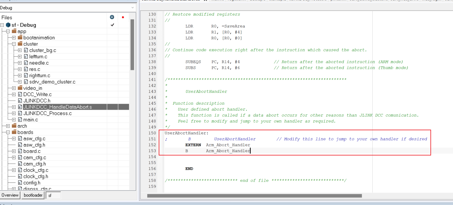
Register JLINKDCC_HandleDataAbort to the Cortex-R5's data abort handler. Modify JLINKDCC_HandleDataAbort to return to the original data abort handler during normal program data aborts. (Optional: This step is to avoid handling data aborts that may occur when the debugger attempts to read invalid memory.)
-
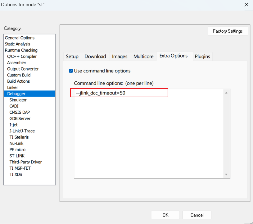
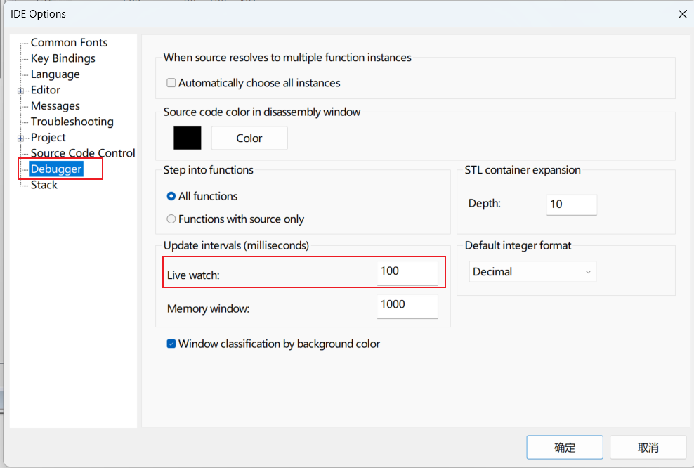
In IAR Options-->Debugger-->Extra Options, set the DCC timeout to --jlink_dcc_timeout=, with a range of 5~5000ms. The default value is 100. Set this to a value greater than the cycle of JLINKDCC_Process().
-
Set the refresh cycle for the Live Watch window. Configure the Live Watch observation window as follows:
-
For systems with an OS, add the following code to periodically retrieve the values of variables added to the Live Watch:
void Task_JLINKDCC_Process(void *pvParameters)
 {
    (void)pvParameters;
    while (1) {
        vTaskDelay(10UL);
        JLINKDCC_Process();
    }
 }

 //Create a task for JLINKDCC polling
 xTaskCreate(Task_JLINKDCC_Process, "Task_JLINKDCC_Process", configMINIMAL_STACK_SIZE, NULL,
                (tskIDLE_PRIORITY + 2), NULL);
-
Test case example:
By adding the variable jlink_var and a pointer variable (which can point to a register address) to the Live Watch window, you can dynamically observe the values of variables or registers during program debugging.
5. Conclusion
In summary, the above methods allow us to observe internal variables of the E3 CPU, facilitating debugging when issues arise.
6. Appendix