
This article mainly introduces how to perform read and write operations on the NSA9260 registers using the MCU: S32K144 and print the values of the registers through a serial port tool.
1. Introduction
1.1 Novosense NSA9260 Boost
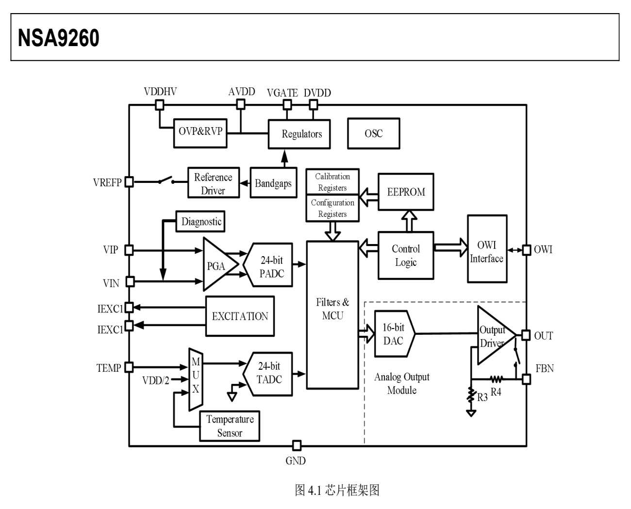
1. NSA9260 is a bridge-type automotive pressure sensor conditioning chip.
2. Supports AEC-Q100 certification.
3. Proprietary OWI communication mode.
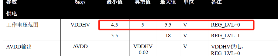
4. Operating voltage range: 4.5~5.5V.
5. Package type: SSOP16.
1.2 NSA9260 Applications
1. Pressure sensors and transmitters.
2. Automotive braking systems.
3. Automotive air conditioning systems.
1.3 NSA9260 Chip Block Diagram
2. Demonstration
2.1 Design Concept
1. Use the MCU (S32K144) to power and communicate with the NSA9260 Sensor.
2. Read and write NSA9260 Sensor registers via the OWI protocol.
3. Read the values of the NSA9260 Sensor registers and print them through the serial port.
2.2 Hardware Resources
1) WPI Echoes (S32K144-Q100).
2) WPI LPClink2 Debugger.
3) NovoSense NSA9260 Sensor.
4) WPI USB Programming Dongle.
Below is the hardware connection diagram: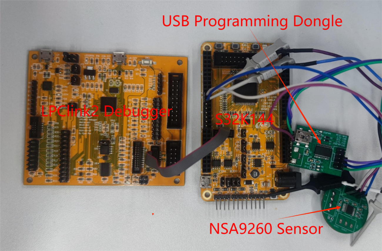
2.3 Software Resources
1) Code development: S32 Design Studio for ARM v2.2.
2) Serial port tool: MobaXterm_Per.
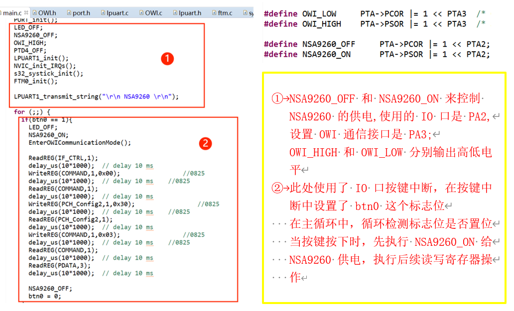
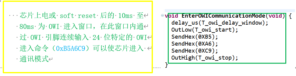
Code snippet:
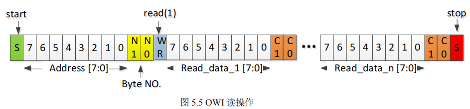
The OWI host needs to send addressing and read/write control information after sending the start condition, including an 8-bit register address, 2-bit byte count control bits, and a 1-bit read/write control bit. The register address indicates the starting address of the register to be read or written (MSB first). The byte count control bits indicate the number of bytes to be read or written consecutively: 00 for 1 byte, 01 for 2 bytes, 10 for 3 bytes, and 11 for 4 bytes. The read/write control bit indicates whether it is a read or write operation: 0 for write, 1 for read.
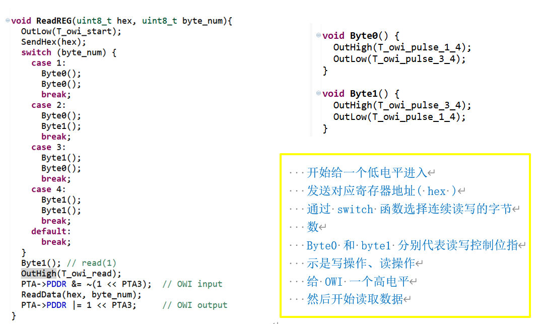
In a read operation, after the OWI host sends the read/write control bit, it pulls the OWI line high for a short period (<1/4 OWI cycle) and then sets the pin to input mode. The chip will start sending the contents of 1/2/3/4 bytes (as determined by the byte count control bits) from the specified register address, along with their 2-bit parity check codes (C1 and C0), as shown in the figure. After receiving all the data, the OWI host regains control of the bus.
Where,
C1 = Read_data[7] ^ Read_data[5] ^ Read_data[3] ^ Read_data[1];
C0 = Read_data[6] ^ Read_data[4] ^ Read_data[2] ^ Read_data[0].
The OWI host can use these parity check bits to determine whether the read data is correct.
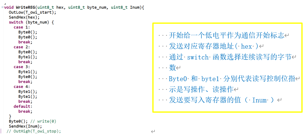
In a write operation, after the OWI host sends the read/write control bit, it continues to send 1/2/3/4 bytes (as determined by the byte count control bits). The data will be sequentially written to the specified register address and subsequent addresses, as shown in the figure.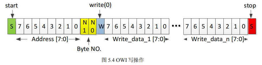
2.4 Serial Port Display
After executing the code, open the serial port display tool. Press the button, and the read/write register values will be displayed as shown below.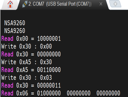
3. Notes
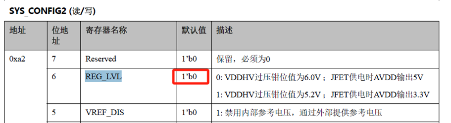
The default value of the NSA9260 REG_LVL register is 0. The supply voltage range is 4.5~5.5V. The voltage supplied to the NSA9260 must be within this range; otherwise, the chip will not function, and communication will fail.
4. Reference
[1] NSA9260X Datasheet Rev1.2CN
Feel free to leave comments below the blog post, and we will respond to your questions promptly. For further inquiries, please contact the ATU department of WPI Group: atu.sh@wpi-group.com
Author: Naib Zhou / Zhou Tiantian