
This article introduces how to leverage the advantages of reflective sensors to simplify and improve the design of miniature optical sensors.
Reflective sensors are excellent tools for designing miniature optoelectronic switches. They are compact and intuitive, making them ideal for simplifying human-machine interaction. These sensors are often hidden behind infrared (IR) lens covers, and they respond quickly when a finger or other object touches the surface of the lens cover.
Optical sensors or reflective sensors can simplify the design process, enabling the creation of intuitive, intelligent, and reliable buttons. They offer a simple yet efficient structure:
- The sensor has an emitter on one end that emits infrared light.
- When a finger or any object approaches, it is illuminated by this light beam.
- The reflected signal generates a photocurrent in the detector on the other end.
These sensors operate invisibly, with no moving parts or friction, resulting in minimal wear and tear. Additionally, optical sensors can be adjusted and fine-tuned to mitigate the effects of moisture, water, dirt, and scratches on the lens cover surface. They can even function efficiently when operated with gloves. However, it is important to note that, like any sensor integrated into an application, achieving optimal results requires addressing various challenges. For optical sensors, these challenges primarily involve environmental and mechanical constraints.
Environmental Challenges
Imagine this: external interferences such as sunlight and typical light sources can create environmental noise for the detector, which needs to be addressed. In such cases, we must consider offset currents caused by peripheral aperture reflections, as well as dirt, water, moisture, or scratches on the lens cover surface. These offset currents can increase the proximity signal, amplifying the total output signal amplitude.
If these factors are not considered during the design phase, the noise signal strength may exceed the set threshold, leading to false detections. To prevent this, sensor designs should minimize the impact of these environmental factors to maintain a proper signal-to-noise ratio.
Mechanical Challenges
For aesthetic purposes, sensors are often hidden beneath infrared lens covers, or the observation apertures of optical sensors are kept as small as possible. Additionally, to accommodate multiple buttons arranged closely together, the sensor's footprint should be minimized. This creates strict mechanical constraints on the sensor's packaging size while also imposing stringent requirements on emission angles and observation characteristics.
Application Scenarios
Having understood the environmental and mechanical challenges involved in designing optoelectronic switches using reflective sensors, let us now explore three specific application scenarios in detail.
01
Touch Switches in Vehicles Operating Under Direct Sunlight
Due to their compact size, optical sensor buttons can be placed anywhere inside a vehicle. However, to adapt to the variable conditions of a vehicle, they must meet high reliability standards. Factors such as temperature fluctuations and sunlight exposure must also be considered.
Sensors can ensure proper orientation by optimizing the aperture to block disruptive sunlight. Additionally, the sensor packaging design should eliminate all troublesome wavelengths of light. This means the sensor only responds to light within the emitter's wavelength range, filtering out most environmental noise.
You can enhance the sensor's functionality by configuring a DC light suppression circuit and a high-pass filter on the detector end, as shown in Figure 1. This circuit ensures that only pulsed emitter signals are detected and amplified.
Figure 1: Detector configured with a DC light suppression circuit and a high-pass filter
02
Optical Button Panels in Confined Spaces
When designing for multiple buttons in a limited space, sensors equipped with emitters are ideal. These emitters can utilize vertical-cavity surface-emitting lasers (VCSELs), which offer high light intensity and strong optical output.
The narrow emission angle of VCSELs significantly reduces offsets caused by the lens cover, making the sensors particularly suitable for operation under transparent materials. Additionally, the light emission pattern and compact size of the sensors allow them to be placed extremely close together. In fact, the arrangement density is only limited by the width of a finger. Thanks to the VCSEL's light emission pattern, you can find a position for the lens cover that minimizes offsets. This optimal point is best determined using a distance curve.
The distance curve (Figure 2) represents the relationship between the sensor's relative output signal and the distance to the lens or cover. Within approximately 2 mm, the signal remains sufficiently low. Ideally, the lens should be kept within this range, with a maximum distance of 2 mm, to minimize offsets and improve the previously mentioned signal-to-noise ratio.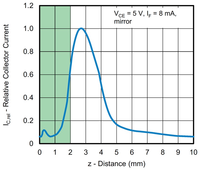
ICrel - Relative Collector Current
z - Distance
Figure 2: Distance curve showing the relationship between the sensor's relative output signal and the distance to the lens or cover.
03
Buttons for Harsh Industrial or Medical Environments
If your goal is to design durable buttons for demanding industrial or medical applications, optical buttons are an excellent choice. Their smooth surfaces lack crevices where dirt can accumulate, making them easy to clean. However, it is crucial that the sensor is not triggered by liquids or dirt.
Moreover, even if a finger is not precisely positioned directly above the sensor, the button should still recognize the press action. Thanks to the wide emission angle of the infrared emitter, optical buttons are less sensitive to dirt on the lens cover surface. This wide-angle emission broadens the distribution area of the light power.
Additionally, the wide-angle emission facilitates the detection of fingers that are not directly placed over the sensor. Importantly, gloves commonly used in such environments do not pose a problem, as the sensor can easily detect them.
Figure 3: A simplified practical button design meeting these standards.
The sensor operates beneath a 3 mm-thick infrared polycarbonate lens cover with a thickness of 2 mm. The aperture design is large enough to accommodate the sensor's wide-angle emission, minimizing offset noise. As shown in Figure 3, the design incorporates the circuit topology from Figure 1 to make it insensitive to sunlight. The emitter's pulse frequency is 5 kHz.
The added high-pass filter ensures that the cutoff frequency is below the pulse frequency, effectively suppressing the typical 50 Hz AC mains noise. The output signal can be directly connected to an analog-to-digital converter for further processing.
Through calibration, the sensor can ignore offsets caused by the aperture. This design is highly stable and offers excellent resistance to false triggers caused by external factors, ensuring extremely reliable performance.